« press release »
Samsung Electronics Envisions Hyper-Growth in Memory and Logic Semiconductors Through Intensified Industry Collaborations at Samsung Tech Day 2022
A new wave of memory solutions and limitless partnership opportunities to bring greater capabilities to data center, server, mobile, gaming and automotive markets. The System LSI Business emphasizes its role as a ‘total solution’ fabless that can optimize solutions for customers through convergence of its wide-range product lineup.
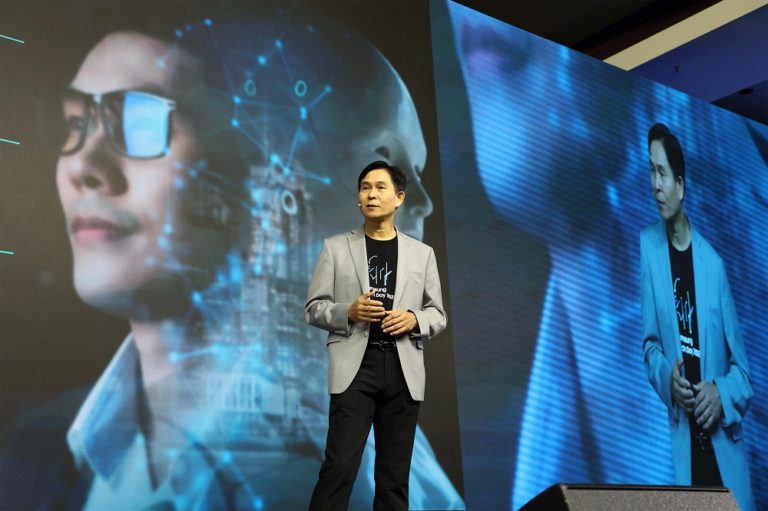
Yong-In Park, President and Head of System LSI Business, is giving his keynote speech at Samsung Tech Day 2022.
Samsung Electronics, a world leader in advanced semiconductor technology, today showcased a series of cutting-edge semiconductor solutions set to drive digital transformation through the decade, at Samsung Tech Day 2022. An annual conference since 2017, the event returned to in-person attendance at the Signia by Hilton San Jose hotel after three years.
This year’s event, attended by more than 800 customers and partners, featured presentations from Samsung’s Memory and System LSI business leaders — including Jung-bae Lee, President and Head of Memory Business; Yong-In Park, President and Head of System LSI Business; and Jaeheon Jeong, Executive Vice President and Head of Device Solutions (DS) Americas Office — on the company’s latest advancements and its vision for the future.
Next-Generation Logic Chips Showcased
Samsung Electronics revealed a number of advanced logic chip technology for the first time at the Tech Day booth, including 5G Exynos Modem 5300, Exynos Auto V920 and QD OLED DDI, which are essential parts of various industries such as mobile, home appliance and automotive.
Chips that were newly released or announced this year including the premium mobile processor Exynos 2200 were also on display, along with the 200MP ISOCELL HP3 — the image sensor with the industry’s smallest 0.56-micrometer (μm)-pixels. Built on the most advanced 4-nanometer (nm) EUV (extreme ultraviolet lithography) process and combined with cutting-edge mobile, GPU and NPU technology, the Exynos 2200 provides the finest experience for smartphone users. The ISOCELL HP3, with a 12 percent smaller pixel size than the predecessor’s 0.64μm, can enable an approximately 20 percent reduction in camera module surface area, allowing smartphone manufacturers to keep their premium devices slim.
Samsung showcased its ISOCELL HP3 in action by showing the attendees of Tech Day the picture quality of photographs taken with a 200MP sensor camera, as well as demonstrating the workings of System LSI’s fingerprint security IC for biometric payment cards that combines a fingerprint sensor, Secure Element (SE) and Secure Processor, adding an extra layer of authentication and security in payment cards.
Memory Business Highlights
In a year marking 30 years and 20 years of leadership in DRAM and NAND flash memory respectively, Samsung unveiled its fifth-generation 10nm-class (1b) DRAM as well as eighth- and ninth-generation Vertical NAND (V-NAND), affirming the company’s commitment to continue providing the most powerful combination of memory technologies over the next decade.
Samsung also emphasized how the company will demonstrate greater resilience through collaborative partnerships in the face of new industry challenges.
“One trillion gigabytes is the total amount of memory Samsung has made since its beginning over 40 years ago. About half of that trillion was produced in the last three years alone, indicating just how fast digital transformation is progressing. As advances in memory bandwidth, capacity and power efficiency enable new platforms and these, in turn, stimulate more semiconductor innovations, we will increasingly push for a higher level of integration on the journey toward digital coevolution.”
— said Jung-bae Lee, President and Head of Memory Business at Samsung Electronics.
DRAM Solutions to Advance Data Intelligence
Samsung’s 1b DRAM is currently under development with plans for mass production in 2023. To overcome challenges in DRAM scaling beyond the 10nm range, the company has been developing disruptive solutions in patterning, materials and architecture, with technology like High-K material well underway.
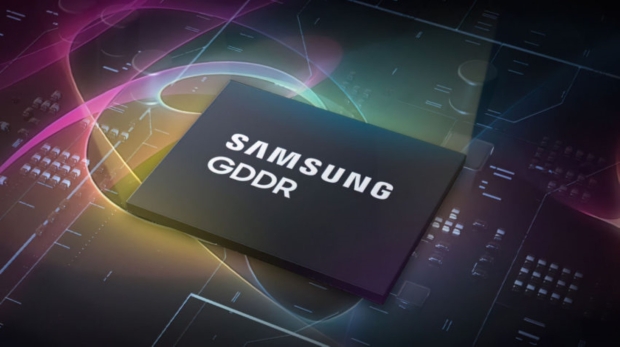
The company then highlighted upcoming DRAM solutions such as 32Gb DDR5 DRAM, 8.5Gbps LPDDR5X DRAM and 36Gbps GDDR7 DRAM that will bring new capabilities to data center, HPC, mobile, gaming and automotive market segments.
Expanding beyond conventional DRAM, Samsung also underscored the importance of tailored DRAM solutions such as HBM-PIM, AXDIMM and CXL that can fuel system-level innovation in better handling the explosive growth of data worldwide.
1,000+ V-NAND Layers by 2030
Since its inception a decade ago, Samsung’s V-NAND technology has progressed through eight generations, bringing 10 times the layer count and 15 times the bit growth. Samsung’s most recent, 512Gb eighth-generation V-NAND features a bit density improvement of 42%, attaining the industry’s highest bit density among 512Gb triple-level cell (TLC) memory products to date. The world’s highest capacity 1Tb TLC V-NAND will be available to customers by the end of the year.
The company also noted that its ninth-generation V-NAND is under development and slated for mass production in 2024. By 2030, Samsung envisions stacking over 1,000 layers to better enable data-intensive technologies of the future.
As AI and big data applications drive the need for faster and higher-capacity memory, Samsung will continue to leapfrog bit density by accelerating the transition to quad-level cell (QLC), while further enhancing power efficiency in support of more sustainable customer operations worldwide.
More Far-Reaching Solutions Amidst Greater Collaboration
Samsung introduced an extensive portfolio of storage solutions spanning data center, enterprise server, mobile, client, consumer and automotive applications. The company highlighted its high-performance, low-power computational storage optimized for AI and how it can contribute to eco-conscious computing. Samsung also presented a new DRAM-less SSD, the PM9C1a, which supports both PCIe 4.0 and 5.0.
Samsung then shared aggressive plans to lead the industry in intelligent mobility solutions. The company discussed its wide-ranging memory offerings designed for every modern automotive function, from in-vehicle infotainment (IVI), autonomous driving (AD) and advanced driver assisted systems (ADAS), clusters and gateways to telematics. Since entering the automotive memory market in 2015, Samsung has been rapidly growing its market presence with the intent of becoming the largest automotive memory provider by 2025.
Reaffirming its overriding goals of enhancing customer value and pursuing a customer-oriented development philosophy, Samsung stressed its intent to further expand its ecosystem partnerships. To stimulate more widespread open innovation, Samsung revealed a key element of its blueprint for greater customer collaboration. The company will open a Samsung Memory Research Center (SMRC) where customers and partners can test and verify Samsung memory and software solutions in various server environments. Beginning with the opening of its first SMRC in Korea in the fourth quarter of this year, Samsung plans to later launch additional hubs in the U.S. and around the world, in collaboration with ecosystem partners like Red Hat and Google Cloud.
« end of the press release »


